
The Ministry of Commerce and Industry has officially notified India’s first semiconductor fabrication facility as a Special Economic Zone in Dholera, Gujarat. Developed by Tata Semiconductor Manufacturing Private Limited in collaboration with Taiwan’s PSMC, the project involves a massive investment of ₹91,000 crore. This development marks a pivotal step in India’s mission to become a global electronics manufacturing hub and reduce its reliance on silicon imports.
The First Mega Fab: Scale and Location
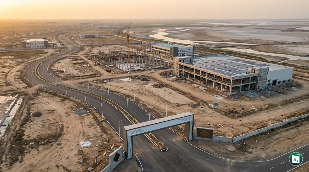
The newly notified Special Economic Zone (SEZ) covers an area of 66.166 hectares within the Dholera Special Investment Region (DSIR). This site is strategically chosen as Dholera is India’s first operational smart city and a key node of the Delhi-Mumbai Industrial Corridor (DMIC). The facility, often referred to as a “mega fab,” is designed to be a high-volume, pure-play foundry that will manufacture chips for a variety of critical sectors.
The project is being spearheaded by Tata Electronics, a subsidiary of the Tata Group. The total layout of ₹91,000 crore makes it one of the largest private sector investments in the history of Indian electronics manufacturing. Once fully operational, the plant is expected to have a manufacturing capacity of up to 50,000 wafers per month.
Strategic Partnership with PSMC
To bring the project to life, the Tata Group has entered into a strategic technical partnership with the Powerchip Semiconductor Manufacturing Corporation (PSMC) of Taiwan. Under this agreement, PSMC will provide the necessary design and construction support, technology licensing, and engineering expertise required for a state of the art fabrication unit.
The plant will focus on manufacturing chips using 28nm, 40nm, 55nm, 90nm, and 110nm nodes. While these are not the smallest nodes used in high-end smartphones, they are the “workhorse” nodes essential for power management circuits, microcontrollers, and display drivers. These chips are vital for the automotive industry, industrial automation, and consumer electronics.
The India Semiconductor Mission (ISM)
This project is the flagship initiative under the India Semiconductor Mission (ISM), which was launched in 2021 with a financial outlay of ₹76,000 crore. The ISM aims to provide fiscal support to companies for setting up semiconductor fabs, display fabs, and compound semiconductors in India. The mission is managed by the Ministry of Electronics and Information Technology (MeitY) through a dedicated nodal agency.
The notification of the SEZ follows significant policy reforms by the Central Government. In June 2025, the government amended the SEZ Rules, 2006, reducing the minimum contiguous land requirement for semiconductor and electronics SEZs from 50 hectares to 10 hectares. This change was specifically aimed at facilitating the rapid setup of high-tech manufacturing clusters like the Dholera fab.
Economic Impact and Import Substitution
India currently imports nearly all of its semiconductor requirements, which is a major contributor to the national trade deficit and a strategic vulnerability. The Dholera fab is a cornerstone of the national import substitution strategy, aimed at building a self-reliant supply chain. By producing chips domestically, India intends to safeguard its industries against global supply chain disruptions like those seen during the pandemic.
The project is also a major employment generator. It is expected to create approximately 21,000 skilled jobs, both direct and indirect. This includes positions for engineers, technicians, and researchers, fostering a high-tech talent pool within the country.
Special Economic Zone Benefits
By being notified as an SEZ, the Tata semiconductor plant will enjoy various fiscal and regulatory benefits. These include:
- Duty-free imports of capital goods and raw materials required for the manufacturing process.
- Single-window clearances for central and state government approvals, reducing bureaucratic delays.
- Tax exemptions on export income for a specified period as per the Special Economic Zones Act, 2005.
- Access to high-quality infrastructure, including consistent power and water supply, which are critical for semiconductor manufacturing.
Key Takeaways
- The Ministry of Commerce and Industry notified India’s first semiconductor fab as an SEZ in Dholera, Gujarat, on April 21, 2026.
- The project is developed by Tata Semiconductor Manufacturing Private Limited (TSMPL) with an investment of ₹91,000 crore.
- Powerchip Semiconductor Manufacturing Corporation (PSMC) of Taiwan is the strategic technical partner for the project.
- The facility spans 66.166 hectares and is located within the Dholera Special Investment Region (DSIR).
- The fab will manufacture chips on 28nm, 40nm, 55nm, 90nm, and 110nm nodes with a capacity of 50,000 wafers per month.
- This initiative is a core part of the India Semiconductor Mission (ISM), launched in 2021 under the Ministry of Electronics and Information Technology.
- The project is expected to generate 21,000 direct and indirect jobs and strengthen India’s import substitution strategy in electronics.