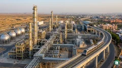

Rajasthan officially entered the global semiconductor ecosystem on May 15, 2026, with the inauguration of its first semiconductor plant and a new Electronics Manufacturing Cluster in Bhiwadi. Established by Sahasra Semiconductors Pvt. Ltd. with an investment exceeding ₹150 crore, this facility is India’s first Small and Medium Enterprise led semiconductor packaging unit to begin commercial production. This milestone marks a critical shift in the country’s high-tech manufacturing landscape by proving that smaller enterprises can actively drive local chip supply chains.
Commercial Semiconductor Production Begins in Bhiwadi
The newly inaugurated facility in the Salarpur industrial area of Khushkhera, within the Bhiwadi region, represents a historic leap for Rajasthan. Developed with an initial investment of over ₹150 crore, the state of the art factory spans 57,000 square feet. To meet the rigorous requirements of semiconductor assembly, the facility is equipped with advanced Class 10,000 and Class 100,000 cleanrooms, which are specialized environments where dust, airborne particles, and temperature are strictly controlled to prevent contamination during chip processing.
The Bhiwadi plant is dedicated to Assembly, Testing, Marking, and Packaging (ATMP), also referred to as Outsourced Semiconductor Assembly and Test (OSAT). This process is the vital final stage of semiconductor manufacturing, where bare silicon dies are packaged into protective casings and rigorously tested before being integrated into electronic devices. The facility will initially focus on packaging high demand products such as eSIMs, Radio Frequency Identification (RFID) chips, LED driver Integrated Circuits (ICs), and memory storage products including Micro SD cards and USB flash drives.
Under the leadership of Sahasra Group Chairman Amrit Lal Manwani and Managing Director Varun Manwani, the plant has commenced operations with a starting annual capacity of 60 million units. Sahasra Semiconductors plans to scale this capacity to between 400 million and 600 million units within the next two to three years as domestic demand grows. This scaling up is expected to create hundreds of high skilled technical jobs and provide local electronics manufacturers with a reliable, indigenous source of packaged components.
The Salarpur Electronics Manufacturing Cluster Ecosystem
The Sahasra facility is housed within the newly developed Salarpur Electronics Manufacturing Cluster (EMC), a specialized industrial enclave spanning 50.3 acres in the Khushkhera-Bhiwadi industrial belt. Developed under the aegis of the Electronic Industries Association of India (ELCINA), the cluster stands as a premier example of public-private cooperation in high-tech infrastructure. ELCINA, established in 1967 and headquartered in New Delhi, is India’s oldest and most influential industry association representing the electronics hardware sector.
This specialized cluster was established with financial and administrative support from the Government of India under the Modified Electronics Manufacturing Clusters (EMC 2.0) scheme. This policy framework was notified by the Ministry of Electronics and Information Technology (MeitY) on April 1, 2020, with the goal of overcoming the infrastructural disabilities of the domestic electronics industry by developing world-class shared facilities. The Salarpur EMC has already attracted planned investments exceeding ₹1,200 crore from a diverse range of companies operating in the semiconductor and electronics supply chains.
The infrastructure in the cluster is designed to lower the entry barriers for new manufacturing units. Key facilities include dedicated high-tension power supply lines, advanced industrial effluent treatment systems, and shared testing laboratories. Additionally, the cluster offers Ready Built Factory (RBF) sheds, which are pre-constructed, fully serviced industrial buildings that allow manufacturers to install their machinery and begin production immediately. This plug-and-play setup significantly reduces the initial capital expenditure and gestation periods, helping Indian enterprises compete more effectively on a global scale.
India’s Semiconductor Policy Matrix: SPECS, EMC 2.0, and ISM
The establishment of Rajasthan’s first semiconductor plant in Bhiwadi is not an isolated success. Instead, it is the direct outcome of a well coordinated federal policy matrix designed to turn India into a self reliant electronics hub. By combining capital incentives, world-class infrastructure support, and targeted strategic backing, these central government initiatives have lowered the entry barrier for domestic manufacturers.
The Sahasra plant was developed under the Scheme for Promotion of Manufacturing of Electronic Components and Semiconductors (SPECS), which was launched by the Ministry of Electronics and Information Technology (MeitY) in April 2020. SPECS provides a financial incentive of 25% of capital expenditure on plant, machinery, cleanroom infrastructure, and research tools, which are heavily capital-intensive. Parallel to this, the Modified Electronics Manufacturing Clusters (EMC 2.0) scheme, notified on April 1, 2020, provided the physical infrastructure by co-funding the ELCINA cluster.
These schemes are further aligned with the overarching India Semiconductor Mission (ISM), which serves as the specialized division within MeitY. While ISM 1.0 was approved in December 2021 with a massive outlay of ₹76,000 crore to attract giant semiconductor fabrication facilities, the recently introduced ISM 2.0 in the FY 2026-27 Union Budget has allocated ₹1,000 crore to build secondary supply chain security. This includes promoting indigenous raw materials, local manufacturing of semiconductor equipment, and creating Indian intellectual property.
| Scheme or Mission | Launch Date | Nodal Agency | Key Objective | Incentives Offered |
|---|---|---|---|---|
| SPECS | April 2020 | MeitY | Promotes manufacturing of electronic components and semiconductors | 25% financial incentive on capital expenditure for plant, machinery, and cleanroom setup |
| EMC 2.0 | April 1, 2020 | MeitY | Establishes Electronics Manufacturing Clusters and Common Facility Centres | Financial assistance up to 50% of infrastructure project costs, including plug-and-play factory sheds |
| ISM 1.0 and 2.0 | December 2021 (ISM 1.0) / February 2026 (ISM 2.0) | India Semiconductor Mission under MeitY | Builds comprehensive local semiconductor manufacturing, display, and design ecosystems | ₹76,000 crore initial outlay (1.0) and ₹1,000 crore (2.0) for supply chains, raw materials, and IP creation |
Why Bhiwadi? The Strategic and Geographic Dimensions
The selection of Bhiwadi, located in the Alwar district of northeastern Rajasthan, as the home for this semiconductor plant is highly strategic. As a vital industrial node within the National Capital Region (NCR), Bhiwadi lies directly along the route of the Delhi-Mumbai Industrial Corridor (DMIC). This geographic positioning places the facility at the center of one of India’s most advanced transport and infrastructure networks.
Because semiconductor manufacturing relies on a fast, temperature-controlled, and reliable logistics system to transport fragile silicon wafers and finished chips, Bhiwadi’s location provides unmatched logistical advantages. The industrial area is directly connected to National Highway 48, which links Delhi and Mumbai. It is also close to domestic cargo terminals, dry ports, and Indira Gandhi International Airport in Delhi, ensuring that imported raw materials and outbound shipments can be moved with minimal delay.
Additionally, the surrounding region encompassing Bhiwadi, Neemrana, and Dharuhera is already one of India’s largest clusters for automobile parts, home appliances, and heavy engineering. This established industrial footprint provides Sahasra Semiconductors with a stable power grid, abundant water resources, and a mature network of local component suppliers. More importantly, it offers direct access to a large pool of highly trained technical talent from premier engineering and vocational institutes across Rajasthan, Haryana, and New Delhi.
Connecting the Dots: Impact on India’s Tech Supply Chains
The successful launch of India’s first Small and Medium Enterprise (SME) led semiconductor plant reveals a deeper, structural evolution in the domestic technology sector. While large scale semiconductor fabrication projects by massive industrial conglomerates capture headlines, they require years to build and billions of dollars in capital. An SME led facility like Sahasra demonstrates that smaller, agile enterprises can quickly establish operational packaging units, democratizing the high-tech supply chain.
This domestic facility provides a critical middle layer that connects raw chip fabrication with final product assembly. By packaging and testing chips locally, India reduces its heavy reliance on imported semiconductors, primarily from East Asia. Local packaging of eSIMs, RFID chips, and LED drivers directly benefits key Indian industries:
- Smart Metering and Power Distribution: The transition to smart power grids relies on secure eSIMs and microcontrollers to monitor and transmit consumption data. Local packaging ensures supply chain security for national infrastructure.
- Consumer Electronics and LED Lighting: Domestic LED driver packaging helps local manufacturers source critical components without facing international shipping delays or currency fluctuations.
- Automotive and IoT: RFID chips packaged in Bhiwadi are essential for automatic toll collection systems like FASTag and the growing Internet of Things (IoT) hardware ecosystem in India.
Analogy · Understanding Semiconductor Packaging Expand analogy
Think of semiconductor manufacturing as the process of publishing a premium book. A chip designer is the author who writes the text. A massive semiconductor fabrication facility, or foundry, is the heavy printing press that stamps millions of words onto large sheets of paper, representing the silicon wafer. However, you cannot sell loose, giant sheets of paper to a reader.
The Outsourced Semiconductor Assembly and Test (OSAT) or packaging plant is like the bookbinder. It carefully cuts the large silicon sheets into individual chip dies, wraps them in a protective plastic or ceramic cover, adds metallic pins so they can connect to a circuit board, and tests every unit for defects. Without the bookbinder, the author’s words remain unreadable. Sahasra Semiconductors acts as this critical bookbinder for India’s electronic devices.
Key Takeaways
- Sahasra Semiconductors Pvt. Ltd. inaugurated Rajasthan’s first semiconductor plant on May 15, 2026, in the Bhiwadi industrial region.
- The new facility is India’s first Small and Medium Enterprise (SME) led Outsourced Semiconductor Assembly and Test (OSAT) plant to start commercial production.
- The factory was set up under the Ministry of Electronics and Information Technology’s (MeitY) SPECS scheme with an investment exceeding ₹150 crore.
- The plant has an initial annual production capacity of 60 million units and plans to scale to between 400 million and 600 million units within three years.
- The plant is located inside the ELCINA Electronics Manufacturing Cluster at Salarpur, developed under MeitY’s Modified Electronics Manufacturing Clusters (EMC 2.0) scheme.
- The Electronic Industries Association of India (ELCINA) was founded in 1967 and is headquartered in New Delhi to support the electronics manufacturing sector.
- The India Semiconductor Mission (ISM) division under MeitY was established in December 2021 (ISM 1.0) with an outlay of ₹76,000 crore, followed by ISM 2.0 in February 2026 with a ₹1,000 crore budget.