

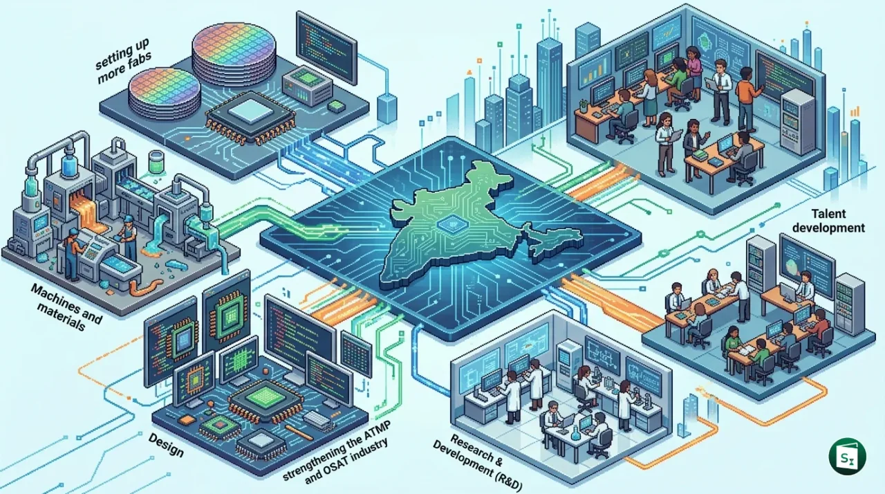
The Union Cabinet chaired by Prime Minister Narendra Modi has approved Semicon 2.0, the second phase of India’s semiconductor programme, with a total outlay of ₹1.27 lakh crore. The scheme aims to build a complete end-to-end semiconductor ecosystem covering chip design, fabrication, packaging, equipment manufacturing, research, and talent development. Semicon 2.0 builds on the momentum of the first phase, under which 12 semiconductor manufacturing units with cumulative investments of over ₹1.64 lakh crore have already been approved.
What Is Semicon 2.0?
Semicon 2.0 is the expanded second edition of the India Semiconductor Mission (ISM), the government’s flagship programme to develop a domestic semiconductor and display manufacturing ecosystem. While the first phase, launched in December 2021 with a ₹76,000 crore outlay, focused primarily on attracting investments for setting up fabrication and packaging facilities, Semicon 2.0 broadens the scope to cover the entire semiconductor value chain.
The government expects Semicon 2.0 to attract total investments of around ₹4 lakh crore and generate semiconductor production worth ₹2 lakh crore during the scheme period. The programme is structured around six pillars that together aim to reduce import dependence, strengthen supply chain resilience, and position India as a reliable player in the global semiconductor network.
The India Semiconductor Mission, established in 2021 as an independent business division within the Digital India Corporation (DIC), serves as the nodal agency for implementing the programme. ISM operates under the Ministry of Electronics and Information Technology (MeitY) and is headed by a Chief Executive Officer. Its advisory board includes global experts from the semiconductor and display industry.
From Semicon 1.0 to 2.0: The Progress So Far
The first phase of the India Semiconductor Mission, launched in December 2021, laid the groundwork by approving four schemes: the Semiconductor Fabs Scheme, the Display Fabs Scheme, the Compound Semiconductors and ATMP/OSAT Scheme, and the Design Linked Incentive (DLI) Scheme. Each offered fiscal support of up to 50% of the project cost on a pari-passu basis.
Under Semicon 1.0, the government approved 12 semiconductor manufacturing units with cumulative investments exceeding ₹1.64 lakh crore. These include 1 silicon semiconductor fabrication unit being set up by Tata Electronics in Dholera, Gujarat, in partnership with Taiwan’s PSMC, 2 compound semiconductor fabrication units, and 9 packaging and testing facilities covering ATMP and OSAT operations.
Of these, Micron Technology (Sanand, Gujarat), Kaynes Semicon (Sanand, Gujarat), and CG Semi (Sanand, Gujarat) have already commenced commercial production. Another unit is expected to begin operations later in 2026. India’s first full-fledged commercial semiconductor fab is scheduled to be commissioned in 2028.
On the design front, 24 semiconductor design projects from startups and MSMEs have been approved for financial support under the Design Linked Incentive (DLI) Scheme, which has an outlay of ₹1,000 crore. Additionally, 105 entities have been granted access to industry-standard Electronic Design Automation (EDA) tools for chip design. Some of these design projects have already completed prototype tape-outs at semiconductor foundries.
The Semicon India Programme has also driven a broader electronics manufacturing boom in India. Electronic goods production rose to about ₹12 lakh crore in 2024-25 from roughly ₹1.9 lakh crore in 2014-15, while mobile phone production increased 28 times to ₹5.45 lakh crore over the same period.
The Six Pillars of Semicon 2.0
Semicon 2.0 is organised around six strategic pillars that collectively address gaps across the semiconductor supply chain.
| Pillar | Focus Area | Key Details |
|---|---|---|
| Design | Chip design and intellectual property | India already has 105 startups developing chips. The scheme aims to deepen the design ecosystem by supporting development of IP, chip designs, and semiconductor systems for strategic and commercial use. |
| Machines and Materials | Equipment and input manufacturing | Companies involved in making semiconductor manufacturing equipment, specialty chemicals, gases, and materials will be incentivised. This lays the foundation for a sustainable and self-reliant precision manufacturing industry. |
| More Fabs | Additional fabrication units | With India’s first silicon fab expected to begin production in 2028, the scheme encourages investments in silicon fabs, compound semiconductor fabs, discrete component fabs, and display fabs. |
| ATMP and OSAT | Assembly, testing and packaging | Global interest in India as an alternative manufacturing destination presents an opportunity to attract advanced packaging technologies. This segment requires lower investment than fabs and can be scaled faster. |
| Research and Development | Advanced technology nodes | While India’s semiconductor journey has started with 28nm to 110nm process nodes, Semicon 2.0 targets more advanced nodes through collaboration with leading research centres in India and abroad. |
| Talent Development | Skilled workforce | 315 universities are currently training students in chip design using industry-standard EDA tools, with around 68,000 students already trained. The programme will deepen this training and add clean room, fab construction, and ecosystem skills. |
Why Semiconductors Matter for India
Semiconductors are the building blocks of all modern electronics, powering everything from smartphones and automobiles to defence systems, medical devices, and artificial intelligence infrastructure. India currently imports most of its semiconductor requirements, making the country vulnerable to global supply chain disruptions.
The Indian semiconductor market was valued at approximately $38 billion in 2023 and is expected to reach $100 to $110 billion by 2030, driven by rising domestic demand for electronics, electric vehicles, 5G equipment, and data centres. Despite this massive market, India’s domestic production has been minimal, creating a strategic imperative to build self-reliance.
A robust semiconductor ecosystem has cascading benefits across multiple sectors. It strengthens national security by ensuring trusted sources of chips for defence and strategic applications. It boosts economic growth by enabling domestic electronics manufacturing, which has already become India’s third-largest export category. It also creates high-value employment across engineering, research, and precision manufacturing.
The programme also aligns with India’s Digital India vision and the broader goal of becoming a global electronics manufacturing hub. India’s electronics manufacturing sector has expanded from about $30 billion in FY15 to $150 billion in FY26, while domestic value addition has increased from 15% to 23% over the same period.
The Way Forward
Semicon 2.0 represents a significant escalation of India’s semiconductor ambitions, but the road ahead remains challenging. Setting up semiconductor fabs requires enormous capital, with a single advanced facility costing $3 to $4 billion. Global competition is intense, with countries like the United States, Taiwan, South Korea, and the European Union offering aggressive incentives to attract chip manufacturing investments.
The government has indicated that Semicon 2.0 is designed to attract investments of around ₹4 lakh crore and lead to semiconductor production worth ₹2 lakh crore during the scheme period. The success of the programme will depend on effective execution, timely approvals, and strong industry partnerships.
Industry experts have suggested that India may need incentives totalling $80 billion by 2035 to build a fully competitive semiconductor ecosystem. However, the phased approach adopted by the government, starting with packaging and assembly before moving to advanced fabrication, is considered pragmatic.
The establishment of the India Semiconductor Research Centre (ISRC) as a world-class research facility and the recently launched Investors Support Portal by ISM are steps in the right direction. The programme’s focus on talent development through university partnerships and EDA tool access is also expected to create a pipeline of skilled engineers for the sector.
Key Takeaways
- The Union Cabinet approved Semicon 2.0 with a total outlay of ₹1.27 lakh crore to develop India’s semiconductor design and manufacturing ecosystem.
- Semicon 2.0 is structured around six pillars: Design, Machines and Materials, More Fabs, ATMP/OSAT, R&D, and Talent Development.
- Under the first phase of the India Semiconductor Mission, 12 semiconductor manufacturing units with cumulative investments of over ₹1.64 lakh crore have been approved.
- The India Semiconductor Mission (ISM) was established in 2021 as an independent business division under Digital India Corporation (DIC) and operates under the Ministry of Electronics and Information Technology (MeitY).
- The first phase of the Semicon India Programme was launched with an outlay of ₹76,000 crore in December 2021.
- India’s first commercial semiconductor fabrication unit, being set up by Tata Electronics in Dholera, Gujarat in partnership with Taiwan’s PSMC, is expected to be commissioned in 2028.