
The Technology Development Board under the Department of Science and Technology has signed an agreement with Bengaluru based BigEndian Semiconductors to provide ₹130 crore for Project VeerAI under the Research Development and Innovation (RDI) Fund. The project has a total cost of ₹260 crore and aims to build an indigenous AI Vision System on Chip for cameras, surveillance and edge devices. The support will help India move a home grown chip design from laboratory validation to full commercial production.
What Is the RDI Fund?
The RDI Fund is a ₹1 lakh crore national fund to give long term and low cost money to private companies for research, development and innovation in sunrise and strategic sectors. The Union Cabinet approved the RDI Scheme on 1 July 2025 for a period of six years, with ₹20,000 crore set aside in 2025-26 for the first year of rollout.
The Department of Science and Technology (DST) serves as the nodal department for the RDI Fund. The fund operates through a Special Purpose Fund (SPF) created inside the Anusandhan National Research Foundation (ANRF). ANRF is the national body set up through the ANRF Act, 2023 to guide research funding across universities, laboratories and industry. The SPF keeps the corpus and sends money through a two tier system to Second Level Fund Managers.
Under the approved framework, the Technology Development Board (TDB) and the Biotechnology Industry Research Assistance Council (BIRAC) act as Second Level Fund Managers. TDB handles technology and engineering projects, while BIRAC, which was set up in 2012 under the Department of Biotechnology and is headquartered in New Delhi, handles biotechnology and life science projects. By July 2026, the government had sanctioned ₹1,000 crore each to TDB and BIRAC, and TDB had approved 22 projects with a total cost of ₹4,744 crore and RDI support of ₹2,192 crore.
What Is the RDI Scheme and Who Can Get Support?
The RDI Scheme is the set of rules under which the RDI Fund gives money. The scheme supports projects at Technology Readiness Level (TRL) 4 and above, which means the basic idea has already been proved in a laboratory and now needs help to become a working product. Support can take the form of low interest loans, equity investment or a dedicated Deep Tech Fund of Funds. Financing is normally limited to 50 percent of the assessed project cost, so the company must bring the remaining share.
| Feature of RDI Scheme | Detail |
|---|---|
| Total corpus | ₹1 lakh crore over six years |
| Nodal department | Department of Science and Technology |
| Fund holder | Special Purpose Fund in ANRF |
| Second Level Fund Managers | TDB, BIRAC, with more funds under review |
| Minimum maturity | TRL 4 and above |
| Focus areas | Energy transition, deep tech including quantum and space, AI in farming health and education, biotech and medical devices, digital economy, and other strategic technologies |
TDB Backs Project VeerAI With Rs 130 Crore Support
The Technology Development Board signed the agreement with BigEndian Semiconductors Pvt. Ltd., Bengaluru for Project VeerAI in early October 2026. TDB will provide ₹130 crore out of the total ₹260 crore project cost. The funding covers exactly half the cost, which matches the RDI rule that public support stays within 50 percent of the assessed cost.
The Technology Development Board will release the money as Optional Convertible Debt (OCD). OCD is a loan that can later turn into company shares under fixed conditions. This structure gives a startup low cost debt at the start, while giving the public funder a chance to hold equity if the technology succeeds.
TDB is a statutory body set up in September 1996 under the Technology Development Board Act, 1995. The Board works under the Department of Science and Technology and is chaired by the Secretary of DST. Its mandate is to help Indian industry turn home grown research into market products or adapt imported technology for wider use in India. TDB has supported more than 440 agreements with funding of over ₹3,261 crore so far. It gives help as soft loans at 5 percent simple interest, equity up to 25 percent of project cost, and grants in rare cases of national importance.
BigEndian Semiconductors is a Bengaluru based fabless chip design startup founded in 2024. A fabless company designs chips but gets the physical manufacturing done at outside foundries. The company builds secure, high performance System on Chip (SoC) products for Vision AI. It raised $3 million in 2024 led by Vertex Ventures and $6 million in May 2026 led by IAN Alpha Fund with Vertex Ventures and IvyCap Ventures. The company has completed tape-out of its first chip, which means the final design has been sent for trial production, and is now moving toward commercial launch. Sunil Kumar is the co-founder and Chief Executive of the company (as of October 2026).
What Is Project VeerAI and the AI Vision Chip?
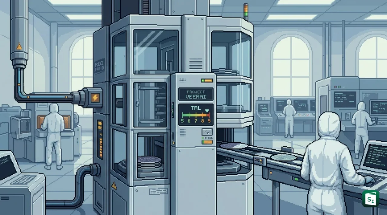
Project VeerAI aims to develop a camera focused AI Vision System on Chip on a sovereign Indian technology platform. A System on Chip is a single chip that packs the processor, memory, image signal unit, input and output controls and security blocks together. It works like a full computer squeezed onto one small piece of silicon.
The VeerAI chip is built for Vision AI, which means it can read and understand video inside the camera itself. The chip can detect movement, recognise faces and number plates, count people and spot unusual activity without sending all the video to a distant cloud server. This on device processing cuts delay, saves internet bandwidth and keeps sensitive video data local.
The first use will be in CCTV and surveillance cameras for cities, offices, transport hubs and critical sites. The same platform can later serve defence systems, cars and drones, factory machines and medical imaging devices. The design follows a Secure by Design approach, where safety features are built into the silicon from the start instead of being added later through software. This matters because cameras and connected devices are often targeted for hacking and data leaks. An Indian chip with Indian intellectual property gives buyers a trusted option and reduces dependence on imported chips.
What Is Technology Readiness Level From TRL 5 to TRL 9?
Technology Readiness Level is a nine point scale to measure how mature a technology is, from a basic idea at TRL 1 to a fully proven product at TRL 9. The scale was first created by the National Aeronautics and Space Administration (NASA) of the United States in the 1980s and is now used by research agencies around the world.
Project VeerAI starts at TRL 5, where the chip parts have been tested together in conditions close to real use. The goal is TRL 9, where the final chip is tested, qualified and sold for regular use in actual cameras and systems. The table below shows the journey in simple terms.
| TRL Stage | What It Means | Status for VeerAI |
|---|---|---|
| TRL 1 to TRL 3 | Basic idea, concept paper, lab proof of concept | Already completed |
| TRL 4 | Small parts tested together in a laboratory | Already completed |
| TRL 5 | Full design tested in a realistic setting | Starting point |
| TRL 6 | Working prototype shown in a realistic end to end setup | To be crossed |
| TRL 7 | Full scale prototype tested in real field conditions | To be crossed |
| TRL 8 | Final system completed and qualified for use | To be crossed |
| TRL 9 | Actual product proved through successful use by customers | Target |
The RDI Fund focuses on TRL 4 and above because this is the stage where private banks hesitate to lend. The technology looks promising but the market risk is still high. Long term and low cost public money bridges this gap, often called the valley of death, and carries the product from prototype to factory output.
India Semiconductor Mission and the National Chip Ecosystem
The India Semiconductor Mission (ISM) is the nodal agency under the Ministry of Electronics and Information Technology to carry out the national chip plan. The government launched the Semicon India Programme (Semicon 1.0) in 2021 with an outlay of ₹76,000 crore to support chip design, fabrication plants, packaging and testing units, display fabs and talent creation. The programme gives 50 percent fiscal support on project cost for approved silicon fabs and for compound semiconductor and ATMP and OSAT plants. ATMP means Assembly Testing Marking and Packaging, while OSAT means Outsourced Semiconductor Assembly and Test. Both refer to the final stage where the silicon wafer is cut, packed and tested.
Building on this base, the Union Cabinet approved Semicon 2.0 on 15 July 2026 with an outlay of ₹1,27,500 crore. Semicon 2.0 rests on six pillars covering chip design, equipment and materials, fabrication plants, advanced packaging, research and development, and talent growth. By September 2026, twelve manufacturing units had been approved and three facilities had started commercial production. The Design Linked Incentive (DLI) Scheme under the mission has approved 24 chip design projects and given design software support to 105 startups and small firms. More than 211 chips had been taped out by 75 academic institutions by April 2026.
Semiconductor companies in India are spread across design hubs in Bengaluru, Hyderabad, Noida and Chennai. Bengaluru hosts design teams of global firms as well as home grown startups such as BigEndian, Tessolve and MosChip. Chip manufacturing companies in India are still in an early stage, with the Dholera plant in Gujarat and new assembly plants leading the pipeline, while the Semiconductor Laboratory (SCL) in Mohali, set up in 1983, provides public research and fabrication support. Project VeerAI fits this national push because it adds an Indian owned product to an ecosystem that has so far been strong in design services but weak in owned silicon products.
Why This Agreement Matters for India
The Technology Development Board agreement shows how the RDI Fund is moving from policy to actual factory level support. TDB received 124 project proposals worth more than ₹25,000 crore in a short window and became the first Second Level Fund Manager to issue calls, sign agreements and release money. In May 2026, TDB signed agreements for five high impact projects in batteries, space, cell therapy, medical devices and drones, and released the first ₹50 crore tranche to Eyestem Research for cell therapy. The VeerAI deal extends this line into semiconductors, which is one of the most import dependent sectors.
For the chip market, the gain is direct. India imports almost all its camera processors today. A home grown Vision AI chip can cut import bills, give Indian camera makers a local supplier and keep video data within trusted hardware. Industry estimates cited by the company place the domestic opportunity for its domain at about $5 billion. If VeerAI reaches TRL 9, Indian firms can buy Indian chips for smart cities, highways, railways, factories and defence posts instead of depending fully on foreign vendors.
For the wider economy, the model is equally important. Long term loans at low rates allow deep tech startups to survive the costly stages of prototyping, testing and certification. TDB support often pulls in private co investment, creates skilled jobs in design and testing, and builds intellectual property that stays in India. The challenge now lies in execution. The team must complete field trials, secure foundry slots for volume production and win buyers against global chip giants. Success will prove that public risk capital can take Indian silicon from laboratory to market.
Key Takeaways
- The Technology Development Board signed support of ₹130 crore for Project VeerAI of BigEndian Semiconductors, with a total project cost of ₹260 crore.
- The funding is sanctioned under the RDI Fund as Optional Convertible Debt and covers 50 percent of the project cost.
- Project VeerAI aims to move an indigenous AI Vision System on Chip from TRL 5 to TRL 9 for full commercial use.
- The RDI Scheme was approved on 1 July 2025 with a corpus of ₹1 lakh crore over six years and operates through a Special Purpose Fund in ANRF.
- The Technology Development Board, set up in 1996 under the TDB Act, 1995, works under the Department of Science and Technology as a Second Level Fund Manager with BIRAC.
- The deal supports the India Semiconductor Mission, under which Semicon 1.0 had ₹76,000 crore and Semicon 2.0 approved in July 2026 has ₹1,27,500 crore.