

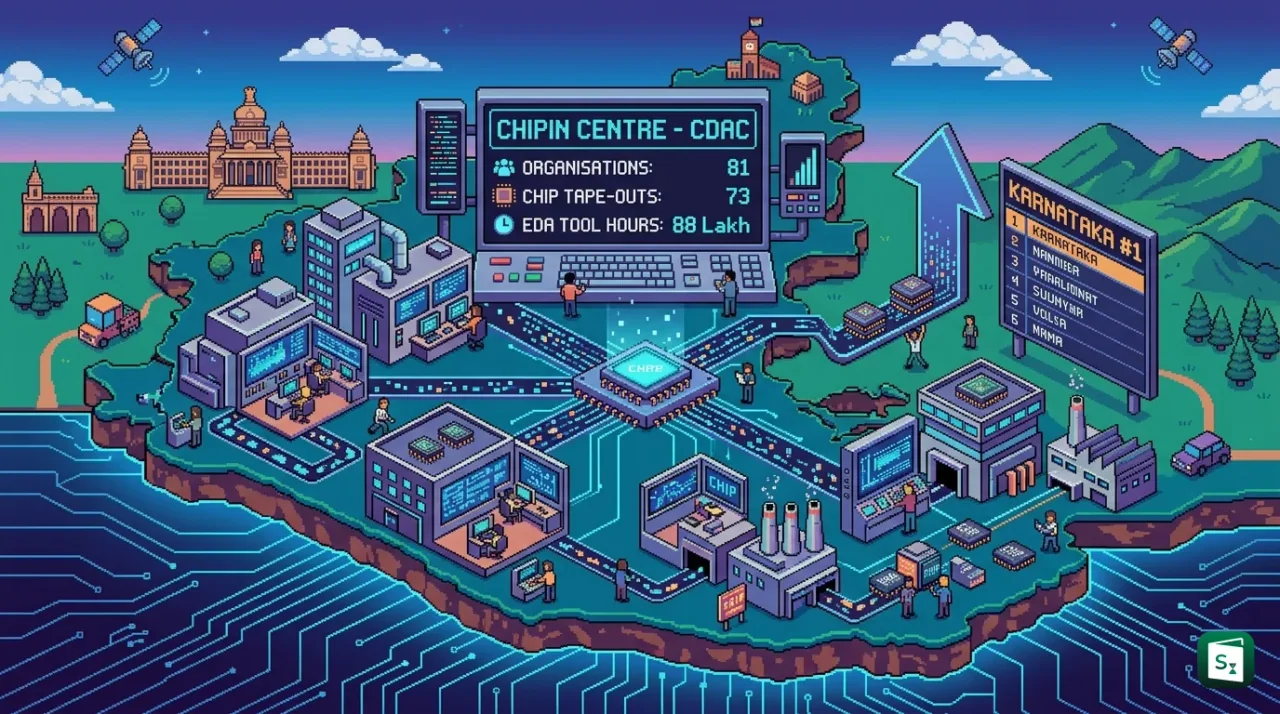
Karnataka has emerged as the leading state in semiconductor support under the ChipIN Centre, a national chip design facility run by the Centre for Development of Advanced Computing (C-DAC) in Bengaluru. According to a dataset released by the Ministry of Electronics and Information Technology (MeitY), the state recorded 81 organisations supported, 73 chip tape-outs, and 88 lakh hours of Electronic Design Automation (EDA) tool usage, all the highest in the country. Tamil Nadu and Telangana followed, showing that India’s chip design ecosystem is now spreading beyond a single hub.
What Is the ChipIN Centre?
The ChipIN Centre is a national, cloud-supported chip design facility set up by MeitY to help fabless chip designers, start-ups, MSMEs, and academic institutions design and fabricate semiconductors. It was launched in 2023 and operates at C-DAC Bengaluru, acting as a one-stop centre for design tools, fabrication access, and prototype testing.
The word “fabless” describes companies that design chips but do not own a fabrication plant. Such firms usually cannot afford costly design software or foundry access on their own. The ChipIN Centre removes that barrier by pooling resources centrally and sharing them across the country.
Where Is the ChipIN Centre Located?
The ChipIN Centre is located at C-DAC Bengaluru in Karnataka, which is why the state naturally hosts the largest share of the facility’s users. A related Virtual Prototyping Lab operates at NIELIT Calicut in Kerala to support VLSI (Very Large Scale Integration) design training. Together, these two facilities form the backbone of India’s shared chip design infrastructure.
What Does the ChipIN Centre Provide?
The Centre offers a full package of design support under one roof:
- Centralised EDA tools from global leaders such as Synopsys, Cadence, and Siemens EDA, covering the entire chip design cycle
- Multi-Project Wafer (MPW) support, which lets several small designs share a single silicon wafer to cut fabrication costs
- Foundry access to Indian facilities such as Semi-Conductor Laboratory (SCL), Mohali, and to overseas foundries
- Design services including fabrication compliance checks, validation, packaging coordination, and prototyping
- A reusable IP core repository and training on EDA tools for students and start-ups
Around 1 lakh individuals from 400 organisations, including about 305 academic institutions under the C2S Programme and 95 start-ups under the DLI Scheme, have used this shared national EDA infrastructure. The EDA tools are offered free of cost, with access provided from 11 leading semiconductor companies.
Karnataka’s Numbers: Why the State Leads
Karnataka tops every major measure of activity under the ChipIN Centre. The gap is widest in EDA tool usage, where the state logged 88 lakh hours, far ahead of the next state. EDA refers to Electronic Design Automation, the software used to design, simulate, and verify a chip before it is manufactured.
The table below shows the leading states in the MeitY dataset:
| State | Organisations Supported | Chip Tape-Outs | EDA Tool Usage |
|---|---|---|---|
| Karnataka | 81 | 73 | 88 lakh hours |
| Tamil Nadu | 79 | 33 | Not specified |
| Telangana | 42 | 28 | Not specified |
| Maharashtra | 32 | 24 | 15 lakh hours |
| Uttar Pradesh | 24 | 21 | Not specified |
| Madhya Pradesh | 24 | 18 | Not specified |
Karnataka’s lead is no accident. Bengaluru is home to one of the world’s largest concentrations of semiconductor design engineers, with offices of global firms such as Qualcomm, Texas Instruments, and Applied Materials. The state also runs India’s major chip design clusters, giving local institutions easy access to mentors, vendors, and industry partnerships.
What Is a Chip Tape-Out and Why Does It Matter?
A chip tape-out is the final stage of the design process, when the completed chip layout is sent to a fabrication plant to be turned into silicon. It marks the point where an idea becomes a physical chip, and it is the most important milestone for any chip designer. Karnataka’s 73 tape-outs represent real, tested designs, not just tool usage.
The MeitY data noted that Karnataka, Tamil Nadu, and Telangana together lead the country in chip tape-outs, EDA access, and overall ecosystem participation. Nationally, the programme has recorded about 3.26 crore hours of EDA tool usage, 254 designs taped out by 67 academic institutions, including 175 designs fabricated domestically at SCL Mohali using 180 nm technology and 79 at overseas foundries.
The Bigger Mission: C2S, DLI, and India Semiconductor Mission
The ChipIN Centre is not a standalone project. It is the shared infrastructure arm of two flagship MeitY schemes, both notified under the umbrella Semicon India Programme. This wider programme has an outlay of ₹76,000 crore to build India’s semiconductor manufacturing and design ecosystem.
The Chips to Startup Programme
The Chips to Startup (C2S) Programme is an umbrella capacity-building initiative launched by MeitY in 2022 with an outlay of ₹250 crore over five years. It works with about 100 academic institutions and R&D organisations to build skilled manpower in VLSI and embedded system design. Its targets include training one lakh students, incubating 25 start-ups, generating 50 patents, and enabling 10 technology transfers. C-DAC Bangalore acts as the programme coordination institution.
Under C2S, the ChipIN Centre collects student chip designs, verifies them, and sends them in batches every three months to SCL Mohali for fabrication in shared wafer runs. This is how students get hands-on experience of the full design-to-silicon journey.
The Design Linked Incentive Scheme
The Design Linked Incentive (DLI) Scheme, launched in December 2021, offers financial incentives and design infrastructure support to domestic companies, start-ups, and MSMEs working on chips, Systems-on-Chip (SoCs), and IP cores. C-DAC is the nodal agency for the scheme.
| Support Category | Benefit | Ceiling |
|---|---|---|
| Product Design Linked Incentive | Reimbursement of up to 50% of eligible expenditure | ₹15 crore per application |
| Deployment Linked Incentive | 6% to 4% of net sales turnover over five years | ₹30 crore per application |
| Design Infrastructure Support | MPW fabrication and post-silicon validation | ₹30 lakh per application |
Both schemes feed into the ChipIN Centre, which is why its usage numbers are a direct indicator of how quickly India’s fabless design ecosystem is growing.
Why Karnataka Is India’s Semiconductor Hub
Karnataka has built the country’s strongest electronics design base over three decades. The state was among the first to frame a dedicated Electronics System Design and Manufacturing (ESDM) policy, and the Karnataka ESDM Policy 2017-22 set up the state’s Semiconductor Venture Fund to support local chip companies.
In 2022, Karnataka became the first state in India to offer a Production Linked Incentive (PLI) for semiconductors, extending incentives to chip design and manufacturing units. A Special Incentives Scheme for the ESDM Sector 2020-2025 added capital subsidies, land subsidies, and patent reimbursement for eligible firms.
The state’s advantage rests on three factors:
- Talent: Bengaluru has one of the world’s largest pools of semiconductor design engineers.
- Industry presence: Global chip design and equipment leaders have major R&D centres in the city.
- National infrastructure: The ChipIN Centre itself is physically located at C-DAC Bengaluru, giving the state the densest access to shared design tools.
This combination makes Karnataka the base for a large share of India’s design-linked activity, even though most wafer fabrication plants are being set up in other states such as Gujarat and Assam.
The Way Forward
The MeitY dataset confirms that India’s chip design programme is producing results, not just announcements. To build on this, C-DAC has invited proposals to set up Regional Support Centres (RSCs) under the ChipIN Centre in six geographic regions of India. These centres will bring EDA tool training and support closer to institutions in states that currently depend on distance access from Bengaluru.
India’s share of global chip design work is already significant, and the country contributes a large share of the world’s semiconductor design engineers. The challenge now is converting design strength into manufactured silicon. With the India Semiconductor Mission 2.0 phase expanding fabrication and assembly units, the designs taped out today under the ChipIN Centre could move from labs into commercial production in the coming years.
Key Takeaways
- Karnataka leads semiconductor support under the ChipIN Centre with 81 organisations, 73 chip tape-outs, and 88 lakh hours of EDA tool usage, as per a MeitY dataset.
- The ChipIN Centre was launched in 2023 and operates at C-DAC Bengaluru, providing free EDA tools, foundry access, and chip fabrication support.
- A chip tape-out is the final design stage where a chip layout is sent to a fabrication plant, making it the key measure of design activity.
- The C2S Programme was launched in 2022 with an outlay of ₹250 crore over five years, while the DLI Scheme was notified in December 2021 with incentives capped at ₹15 crore and ₹30 crore per application.
- The Semicon India Programme has a total outlay of ₹76,000 crore, covering chip design, fabrication, and assembly.
- Karnataka was the first Indian state to offer a PLI for semiconductors in 2022, supported by its ESDM policies and Bengaluru’s large design talent pool.