
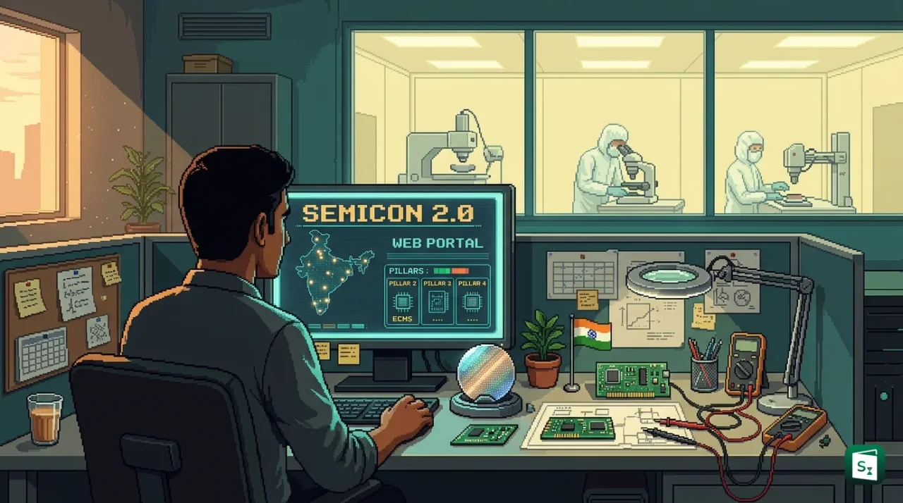
Union Minister Ashwini Vaishnaw launched the Semicon 2.0 web application portal in New Delhi on 6 November 2026 under the second phase of the Semicon India Programme. The portal opens applications for chip equipment and materials, new fabrication plants, and chip packaging units. At the same event, the government approved 12 new projects worth ₹7503 crore under the Electronics Components Manufacturing Scheme.
What Is Semicon 2.0?
Semicon 2.0 is the second phase of the Semicon India Programme, India’s national mission to design and manufacture semiconductor chips within the country. The Union Cabinet approved Semicon 2.0 on 15 July 2026 with a financial outlay of ₹127500 crore. The India Semiconductor Mission (ISM) is the nodal agency that runs the programme under the Ministry of Electronics and Information Technology (MeitY).
Semicon 2.0 builds on the first phase, which focused mainly on chip factories and packaging units. The new phase covers the full chip value chain, from raw materials to finished chips. It rests on six strategic pillars across 10 categories. Projects will generally run for up to six years, while applications will remain open for three years.
| Pillar | Focus Area | What It Covers |
|---|---|---|
| Pillar 1 | Design of chips | Chip IPs, chips, Systems on Chips and deployment incentive |
| Pillar 2 | Machines and materials | Chip making equipment, chemicals, gases and materials |
| Pillar 3 | Setting up more fabs | Silicon, compound, discrete and display fabs |
| Pillar 4 | ATMP and OSAT industry | Advanced and conventional chip packaging |
| Pillar 5 | Research and Development | Advanced nodes and new chip technologies |
| Pillar 6 | Talent development | Design, factory and clean room skills |
Under the design pillar, the goal is to make India a creator of chip design intellectual property and not only a user of foreign designs. Startups and small firms will get seed money, access to design tools and deployment linked incentives to meet tape out costs. Under the machines and materials pillar, firms that make precision tools, specialty chemicals and ultra pure gases will get support to cut import dependence and join global supply chains.
Why the New Portal Matters for Pillars 2, 3 and 4
The Semicon 2.0 web application portal is the online window through which companies apply for support. MeitY issued notifications for all six pillars on 31 August 2026. With the launch on 6 November 2026, applications are now live for three pillars.
Pillar 2 invites makers of semiconductor machinery, materials, chemicals and gases. The aim is to attract at least three large equipment makers and five chemicals and gases firms to India. Pillar 3 invites proposals for new fabrication plants, called fabs. These include silicon fabs, compound semiconductor fabs, discrete component fabs and display fabs. Silicon fabs based on CMOS technology will get 40 percent of project cost as fiscal support, while other fabs will get 35 percent on a pari passu basis, which means government funds are released in step with company spending.
Pillar 4 seeks to strengthen ATMP, which means Assembly, Testing, Marking and Packaging, and OSAT, which means Outsourced Semiconductor Assembly and Test. ATMP is the process of cutting a ready wafer into small dies, joining each die to a package, sealing it and testing it. OSAT is the business model in which a specialist firm does this work on contract for chip designers. Advanced packaging will get 35 percent support and conventional packaging will get 25 percent.
Together, these three pillars fill the missing middle of the chip chain. Design alone cannot succeed without local machines, clean fabs and packaging lines.
From Semicon 1.0 to Semicon 2.0: How India’s Chip Mission Has Grown
The Semicon India Programme was first approved in December 2021 with an outlay of ₹76000 crore. The India Semiconductor Mission was set up in 2021 as a specialised division within the Digital India Corporation to run it. The mission acts as the single window for appraisals, approvals and coordination with state governments, which provide land, water, power and extra incentives.
Under this first phase, 12 manufacturing units were approved with total investment of more than ₹1.64 lakh crore across six states. These include one silicon fab, one silicon carbide fab, one gallium nitride micro LED display fab and nine packaging units. The Tata Electronics fab with Taiwan’s PSMC at Dholera in Gujarat is the flagship silicon fab, with commercial output expected around 2028. Five units had started commercial production by October 2026, including Micron at Sanand, Kaynes at Sanand, CG Semi at Sanand, CDIL at Mohali and Suchi at Surat.
Progress on design and talent has been strong. Twenty four design projects from startups and small firms received financial help, while 105 startups received access to industry standard Electronic Design Automation (EDA) tools, which are software suites used to design and verify chips. Over 68000 students across 315 universities were trained in complex chip design. Semicon 2.0 will deepen this base, support research on more advanced nodes beyond the current 28nm to 110nm range, and expand clean room and factory training with industry.
Twelve New ECMS Approvals Worth ₹7503 Crore
The Electronics Components Manufacturing Scheme (ECMS) builds the domestic supply chain for electronics parts and materials. The Union Cabinet approved ECMS on 28 March 2025 and MeitY notified it on 8 April 2025 with an initial outlay of ₹22919 crore. The Union Budget for 2026 to 27 raised the outlay to ₹40000 crore. The scheme runs for six years and offers turnover linked, capital expenditure and hybrid incentives tied to investment, sales and jobs.
The 12 new approvals are the sixth tranche under the scheme. They involve investment of ₹7503 crore, expected production of ₹39045 crore and 7127 direct jobs. The projects cover 10 target segment products and are spread across Gujarat, Karnataka, Madhya Pradesh, Maharashtra, Punjab, Tamil Nadu and Uttar Pradesh. Approvals for copper foil, cathode active material and specialty ceramics have been given for the first time under ECMS.
| Category | Product | Approved Company |
|---|---|---|
| Components (4) | Multi layer PCB | NeST ICELR Private Limited |
| Components (4) | Relays | TDConnex Chennai Private Limited |
| Components (4) | Heat sinks | Modern Automotives Limited |
| Components (4) | Specialty ceramics | Voltix Semicon Private Limited |
| Supply chain (5) | Copper foil for laminates and lithium ion cells | Indo Asia Copper Limited |
| Supply chain (5) | Anode material for lithium ion cells | TACC Limited |
| Supply chain (5) | Cathode active material | Vidyuta Materials Private Limited |
| Supply chain (5) | Polypropylene film for capacitors | Enerfolie LLP |
| Supply chain (5) | Camera rim | Surface Modification Technologies Private Limited |
| Capital goods | Precision molds, power systems and factory automation | TDConnex, Rockwell Automation India and Wipro Pari Robotics |
Large upstream bets stand out. Indo Asia Copper will invest ₹3546 crore in Gujarat for copper foil. TACC will invest ₹2438 crore in Madhya Pradesh for anode material. Vidyuta Materials will invest ₹399 crore for cathode active material. Copper foil feeds copper clad laminates for printed circuit boards and lithium ion cells, while anode and cathode materials form the core of batteries.
With this tranche, total ECMS approvals have reached 118 applications covering 34 products across 16 states. Total expected investment is ₹77051 crore, with projected production of ₹573146 crore and 81755 direct jobs. Nearly half the approved units belong to micro, small and medium enterprises. Earlier, 106 applications worth ₹69548 crore had been cleared.
What Is a Semiconductor Chip and Why Fabs and Packaging Matter
A semiconductor chip is a tiny block of material, usually silicon, that controls electric current to process, store and sense data. Semiconductors conduct electricity partly, unlike conductors that conduct fully and insulators that block it. Common materials include silicon, silicon carbide and gallium nitride. Every phone, car, satellite and power system uses these chips.
A chip passes through three broad stages. First comes design, where engineers draw and test circuits using EDA software. Second comes fabrication in a fab, where the design is printed on silicon wafers in ultra clean rooms using light based patterning. This is the most capital heavy step, as a single fab costs thousands of crores. Third comes packaging and testing in ATMP or OSAT units, where wafers are cut into dies, sealed into protective bodies and checked for quality.
India’s strategy follows this order. The country is strong in design, with a large share of global chip design work done by Indian engineers. It started manufacturing with packaging units, which need less capital and can start faster, and is now moving to full fabs. Local copper foil, specialty ceramics, gases and automation tools will raise domestic value addition, cut imports and make supply chains more resilient.
Key Takeaways
- The Semicon 2.0 web application portal was launched on 6 November 2026 for Pillars 2, 3 and 4.
- Semicon 2.0 was approved on 15 July 2026 with an outlay of ₹127500 crore under the India Semiconductor Mission.
- The first phase approved 12 units worth over ₹1.64 lakh crore, with five units in commercial production by October 2026.
- The 12 new ECMS approvals involve ₹7503 crore investment, ₹39045 crore production and 7127 direct jobs.
- Total ECMS approvals now stand at 118 applications across 16 states with ₹77051 crore investment and 81755 jobs.