

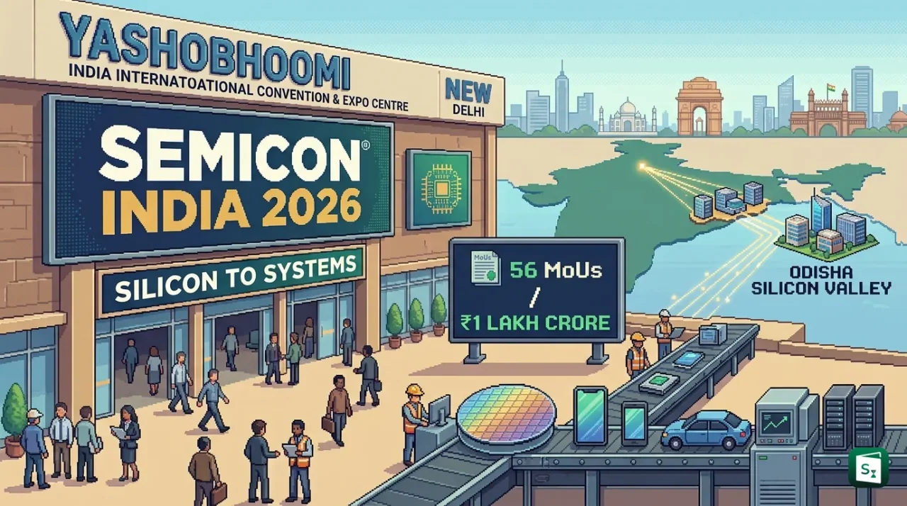
Prime Minister Narendra Modi inaugurated the fifth edition of SEMICON India 2026 on 17 September 2026 at Yashobhoomi in New Delhi. The three day event, held from 17 to 19 September under the theme Silicon to Systems: Building the Ecosystem, brought together more than 600 exhibitors from 52 countries and closed with 56 MoUs. The announcements included investment commitments of around ₹1 lakh crore under Semicon 2.0 and a plan for an Odisha Silicon Valley at Naraj in Cuttack.
What Is a Semiconductor and What Is SEMICON India?
A semiconductor is a material, usually made from silicon, whose ability to carry electricity lies between a conductor like copper and an insulator like rubber. A semiconductor chip is a tiny plate of this material packed with millions of miniature switches that process and store data. These chips power mobile phones, cars, computers, medical devices, defence systems and satellites.
SEMICON India is India’s flagship annual conference and exhibition for the chip ecosystem. The Ministry of Electronics and Information Technology (MeitY) organises SEMICON India through the India Semiconductor Mission (ISM) in partnership with SEMI, which stands for Semiconductor Equipment and Materials International, the global industry body for chip equipment and materials makers. The event brings chip makers, equipment suppliers, chemical firms, designers, startups, researchers, investors and policymakers to one platform to discuss manufacturing, design, supply chains and jobs.
SEMICON India 2026: Dates, Venue, Theme and Scale
SEMICON India 2026 was the fifth edition of the event. The Ministry of Electronics and Information Technology held SEMICON India 2026 from 17 to 19 September 2026 at Yashobhoomi, which is the India International Convention and Expo Centre at Dwarka Sector 25 in New Delhi. Yashobhoomi is India’s largest convention and exhibition complex, with a convention centre that can host about 11,000 delegates and large exhibition halls connected by a central foyer.
The theme for SEMICON India 2026 was Silicon to Systems: Building the Ecosystem. The theme signals a shift in focus. India is no longer asking only whether it can make chips. It is now trying to build everything around chips, from silicon wafers and chemicals to chip design, fabrication, packaging, electronics products and skilled workers. A special Value Chain Experience at the venue showed this full journey from sand to silicon to finished systems.
| SEMICON India 2026 at a Glance | Details |
|---|---|
| Dates | 17 to 19 September 2026 |
| Venue | Yashobhoomi, Dwarka, New Delhi |
| Organisers | ISM, MeitY and SEMI |
| Exhibitors | More than 600, including about 300 international firms |
| Countries | 52 countries, with six country pavilions for Japan, South Korea, Malaysia, Netherlands, Singapore and Sweden |
| Indian participation | 12 state pavilions, Startup Pavilion, Workforce Development Zone and student hackathon |
| Registrations and footfall | 51,656 registrations and cumulative footfall of about 40,000 |
| Speakers and leaders | More than 150 speakers and more than 400 executives |
The Prime Minister inaugurated the exhibition on 17 September and interacted with industry participants. Sessions during the three days covered chip design using artificial intelligence, advanced packaging, manufacturing equipment, materials, supply chain strength, research and workforce development.
India Semiconductor Mission: From Semicon 1.0 to Semicon 2.0
The India Semiconductor Mission (ISM) is the nodal agency for India’s chip programme. The Union Cabinet approved the Semicon India Programme on 15 December 2021 with an outlay of ₹76,000 crore. The government set up ISM as an independent business division within the Digital India Corporation under MeitY. ISM appraises project proposals and supports schemes for fabrication plants, packaging plants and chip design.
Semicon 1.0 focused on creating the first base for manufacturing. It offered up to 50 percent fiscal support on a matching basis for silicon fabs, display fabs, compound semiconductor plants and for ATMP and OSAT units. ATMP stands for Assembly, Testing, Marking and Packaging, while OSAT stands for Outsourced Semiconductor Assembly and Test. Both terms refer to plants where silicon wafers made in a fab are cut, assembled into protective covers and tested before use. Semicon 1.0 also included the Design Linked Incentive (DLI) scheme for startups and chip design firms. Under this phase, 12 projects were approved across six states with investment commitments of more than ₹1.64 lakh crore. By September 2026, five units had started commercial production, including units linked to Micron, Kaynes, CG Semi, CDIL Semiconductor in Mohali and Suchi Semicon in Surat.
The Union Cabinet approved Semicon 2.0 on 15 July 2026 with a much larger outlay of ₹1,27,500 crore for six years. The Prime Minister said the mission budget had grown from $8 billion in the first phase to $13.5 billion in the second phase. While the first phase built fabs and packaging plants, Semicon 2.0 covers the full supply chain, from equipment and gases to design ownership, research and trained workers.
| Feature | Semicon 1.0 | Semicon 2.0 |
|---|---|---|
| Launch | December 2021 with ₹76,000 crore | July 2026 with ₹1,27,500 crore |
| Main focus | First fabs, display fab, ATMP and OSAT, design incentive | Full ecosystem including equipment, materials, more fabs, advanced packaging, research and talent |
| Six pillars | Not structured as six pillars | Design, machines and materials, new fabs, advanced packaging, research and talent development |
| Support pattern | Up to 50 percent of project cost for fabs | 30 to 40 percent for most plant types and up to 75 percent for research and talent projects |
| Progress | 12 projects approved, five in commercial production | Investment commitments of around ₹1 lakh crore reported at SEMICON India 2026 |
Where Are Semiconductor Plants in India?
A chip factory is called a fab, which is short for fabrication plant. A fab prints tiny circuits on round silicon plates called wafers. After that, a packaging plant cuts the wafer into individual chips, packs them and tests them. India is building both types of units, along with research labs that design and test chips.
The Semiconductor Laboratory (SCL) at Mohali in Punjab is India’s key public lab for chips. SCL operates a 180 nanometre CMOS fab, where CMOS stands for Complementary Metal Oxide Semiconductor, a common method to build chips, and works with the Indian Space Research Organisation (ISRO). The Vikram Sarabhai Space Centre designed the VIKRAM3201 chip, which is India’s first fully indigenous 32 bit microprocessor for launch vehicles. SCL fabricated this chip, and ISRO validated it in space on the PSLV-C60 mission. The chip can work in extreme temperatures from minus 55 degrees to plus 125 degrees Celsius.
| Plant or Lab | Location | What It Makes |
|---|---|---|
| Tata Electronics with PSMC Taiwan | Dholera, Gujarat | 300 millimetre fab with capacity up to 50,000 wafers per month for power, display driver and microcontroller chips, investment up to ₹91,000 crore |
| Tata Electronics OSAT | Jagiroad, Assam | Assembly and test plant with investment of ₹27,000 crore using wire bond, flip chip and system packaging |
| Micron Technology | Sanand, Gujarat | ATMP plant of $2.75 billion for memory chips including DRAM, which stands for Dynamic Random Access Memory, and NAND flash memory, spread over 93 acres |
| CG Semi, Kaynes Semicon | Sanand and other sites in Gujarat | Packaging and test units, among the first to start commercial production |
| CDIL Semiconductor | Mohali, Punjab | Discrete devices, commercial line inaugurated in September 2026 |
| Suchi Semicon | Surat, Gujarat | Packaging unit that produced India’s first commercial QFN chip, where QFN stands for Quad Flat No-lead, a compact chip package, with eInfochips |
| SiCSem and 3D Glass Solutions | Odisha | Silicon carbide fab with 60,000 wafers per year and glass substrate packaging unit |
Tata Electronics confirmed at SEMICON India 2026 that work on the Dholera fab and the Jagiroad plant is on track. The company signed seven MoUs for wafer manufacturing, advanced packaging, supply of photoresists and chemicals, localisation of materials and talent development with firms including Fujifilm, JSR Corporation, Nexperia and BESI Singapore.
56 MoUs and Investment Push at SEMICON India 2026
SEMICON India 2026 closed with 56 MoUs, announcements and strategic initiatives. These covered chip design, fabrication, advanced packaging, equipment and materials, power electronics, artificial intelligence, high performance computing, research, logistics, commercial use of lab research, skilling and global cooperation. The agreements linked manufacturers, material suppliers, design firms, universities and training bodies. The aim was to fill gaps around a fab, such as pure gases, chemicals, wafers, masks, testing labs and repair centres for costly machines.
The central government reported investment commitments of around ₹1 lakh crore under Semicon 2.0 during the event. Applied Materials shared an India Vision to invest $5 billion over ten years and expand its supply chain capacity in India tenfold by 2035. Other key outcomes included India’s first commercial QFN chip by Suchi Semicon and eInfochips, use of the India designed SenseSoC-200 chip in smart meters, six ChipIN regional centres for design support and the HORIBA India KOACH Experience Centre for training.
The event also pushed startups and talent. A Startup Pavilion and a Workforce Development Zone showcased young firms and training needs. The SEMICON India Hackathon 2026 invited students to solve chip related problems. Officials noted that India already accounts for about 20 percent of the world’s chip design workforce, with large design centres of global firms in Bengaluru, Hyderabad and Noida, but needs more experienced workers for fabs and packaging plants.
Odisha Silicon Valley at Naraj in Cuttack
Odisha Chief Minister Mohan Charan Majhi announced at SEMICON India 2026 that the state will develop an Odisha Silicon Valley on 870 acres at Naraj near Cuttack. The hub will host semiconductor, electronics and information technology projects. Naraj lies on the Cuttack Bhubaneswar corridor with road links to national highways and multimodal access to the Paradip and Dhamra ports. Its closeness to the Mahanadi river matters because chip and packaging units need large and steady supplies of water and power.
Odisha said it received investment proposals worth about ₹23,600 crore with potential for 6,100 jobs during the event. The state has aligned its semiconductor policy with Semicon 2.0 and offers 25 percent additional fiscal support over ISM support for equipment, gases, raw materials and supply chain projects, along with help for relocation, skilling, internships, patents and research. Odisha has approved two ISM backed projects, a silicon carbide fab and packaging unit by SiCSem and an advanced glass substrate packaging unit by 3D Glass Solutions, and has cleared five state projects worth about ₹11,000 crore. The state also signed a letter of intent with QuadQuantum for silicon carbide substrate wafers.
Why Semiconductors Matter for India
Semiconductors sit at the base of modern growth. They run phones, electric vehicles, solar systems, telecom networks, medical tools and space systems. India’s electronics production has grown about sixfold in ten years, while electronics exports have grown about eightfold. Stable policies and rising domestic demand for chips make local manufacturing important for supply security and jobs.
For India, the strategy has two arms. The first arm is to build sovereign strength in design, packaging and select manufacturing where India has an edge. The second arm is to partner with trusted global firms for equipment, materials and technology where imports remain faster and cheaper. Foreign Secretary Vikram Misri said at SEMICON India 2026 that self reliance does not mean making everything at home. It means building discipline in chosen areas and forming partnerships based on trust, predictability and long term investment.
Key Takeaways
- The 5th SEMICON India was held from 17 to 19 September 2026 at Yashobhoomi in New Delhi under the theme Silicon to Systems: Building the Ecosystem.
- SEMICON India 2026 was organised by ISM and MeitY with SEMI and recorded 600 plus exhibitors, 52 countries and 56 MoUs.
- Semicon 2.0 was approved on 15 July 2026 with an outlay of ₹1,27,500 crore against ₹76,000 crore for Semicon 1.0 launched in 2021.
- Investment commitments of around ₹1 lakh crore under Semicon 2.0 were reported at SEMICON India 2026.
- The Odisha Silicon Valley will come up on 870 acres at Naraj in Cuttack, with proposals worth ₹23,600 crore and 6,100 jobs announced in Odisha.
- Anchor projects include the Tata PSMC fab at Dholera, the Tata OSAT at Jagiroad and the Micron ATMP at Sanand, while VIKRAM3201 is India’s first indigenous 32 bit space microprocessor.