
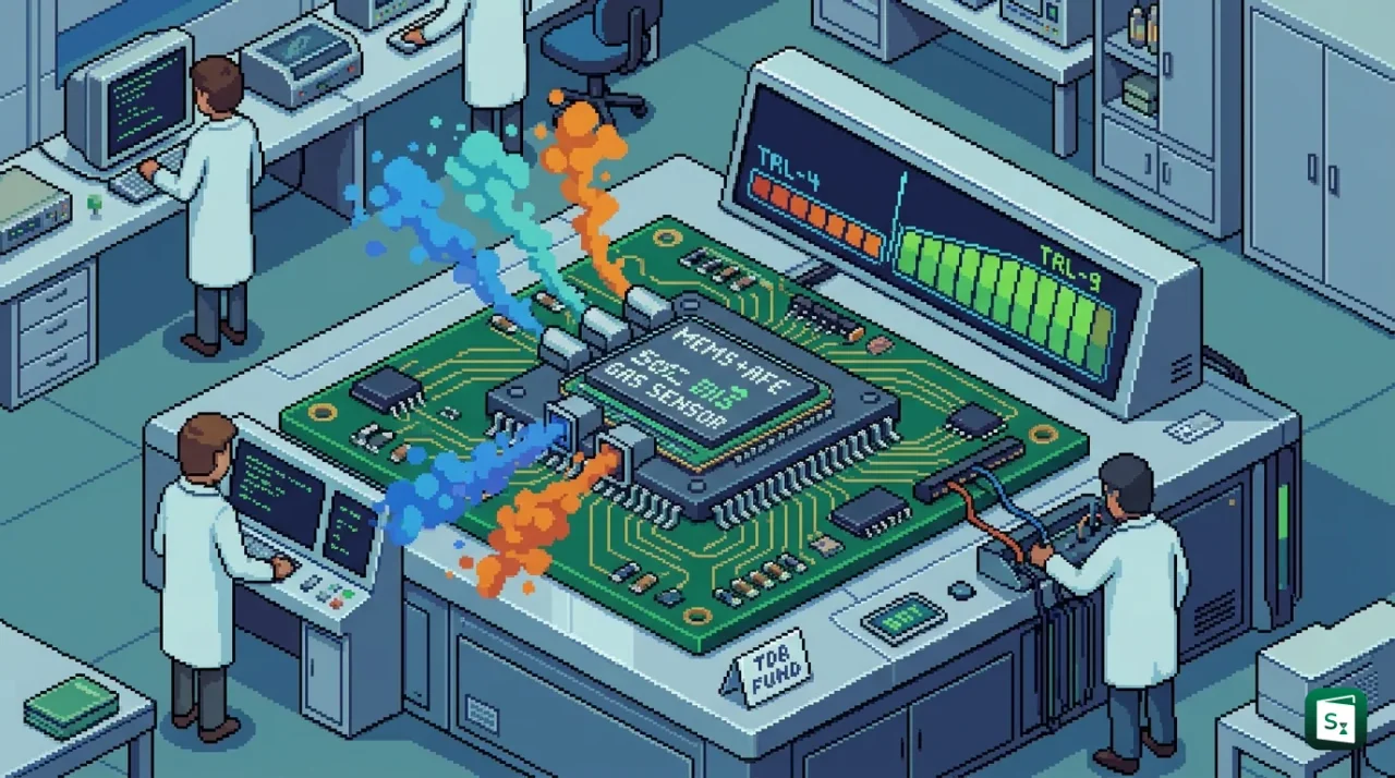
The Technology Development Board signed an agreement on 29 September 2026 with Multi Nano Sense Technologies of Nagpur to support an indigenous multi gas sensor chip. The Board will provide ₹37.51 crore from the Research Development and Innovation (RDI) Fund for a project with a total approved cost of ₹75.02 crore. The project will take a Platform MEMS plus Analog Front End System on Chip from laboratory validation to a market ready product, strengthening domestic capability in sensors and semiconductors.
What Is the RDI Fund?
The Research Development and Innovation Fund is a ₹1 lakh crore national fund to give long term, low interest loans to private companies for research in sunrise and strategic sectors. The Department of Science and Technology implements it through a Special Purpose Fund in the Anusandhan National Research Foundation.
The Union Cabinet approved the Research Development and Innovation (RDI) Scheme on 1 July 2025 with a total corpus of ₹1 lakh crore to be spent over six years, including ₹20,000 crore in 2025-26. The Anusandhan National Research Foundation (ANRF) acts as the custodian of the money through a Special Purpose Fund. The Department of Science and Technology (DST), which was set up in May 1971, serves as the nodal department for implementation.
The scheme uses a two tier system. In the first tier, the Special Purpose Fund holds the corpus. In the second tier, the money flows to Second Level Fund Managers (SLFMs) as long term concessional loans. The SLFMs then fund eligible companies, startups and industry led research projects. The Technology Development Board (TDB) and the Biotechnology Industry Research Assistance Council (BIRAC) were designated as SLFMs and issued calls for proposals in February 2026.
The fund has four clear aims. It encourages private firms to increase research in sunrise domains and in areas linked to economic security and self reliance. It finances transformative projects at Technology Readiness Level (TRL) 4 and above, which means the basic proof of concept is already proven in a laboratory. It supports acquisition of critical technologies of high strategic value. It also helps create a dedicated Deep Tech Fund of Funds.
This design responds to a long standing gap. India’s Gross Expenditure on Research and Development (GERD) is about 0.64 percent of GDP, with the public sector contributing about 60 percent and the private sector only about 35 to 36 percent. In leading innovation economies, private firms contribute more than 70 percent. The RDI Fund offers patient capital, mainly as long term loans at low or nil interest and in some cases as equity for startups, to reduce risk for deep technology work that banks normally avoid.
What Is a MEMS Sensor and How Does It Work?
A Micro Electro Mechanical Systems sensor is a microscopic device that combines tiny moving mechanical parts with electronics on a single silicon chip. It senses a change in its surroundings, such as movement, pressure or gas, and converts that change into a small electrical signal for processing.
The full form of MEMS is Micro Electro Mechanical Systems. These devices are built with the same fabrication methods used for integrated circuits, but they add moving structures such as membranes, cantilevers and micro channels. Their size typically ranges from a few micrometres to a few millimetres. Because they are very small, they consume little power, cost less in large volumes and can be easily combined with digital circuits.
A MEMS sensor works in three simple steps. First, the micro structure reacts to the outside world. For example, a membrane bends under gas pressure or a proof mass shifts under acceleration. Second, a process called transduction changes this movement into an electrical signal, often through change in capacitance or through piezoelectric materials that produce charge when pressed. Third, an Application Specific Integrated Circuit (ASIC), which is a custom chip designed for one task, cleans and amplifies this weak analog signal and converts it into stable digital data.
MEMS devices already form a large family. Common members include accelerometers that detect motion, pressure sensors, microphones, tilt sensors and inertial measurement units (IMUs) that combine accelerometers and gyroscopes for navigation. A MEMS gas sensor applies the same idea to chemistry. Its sensing layer reacts when target gas molecules touch it, and the electronics read that reaction as a change in resistance, heat loss or capacitance to estimate gas type and concentration.
What Is the New Multi Gas Sensor Project?
The Technology Development Board signed the agreement with Multi Nano Sense Technologies Private Limited, a deep technology company based in Nagpur, Maharashtra, on 29 September 2026. The Board will provide ₹37.51 crore as Optionally Convertible Debt (OCD), which is a loan that can later be converted into company shares if needed. The total approved project cost is ₹75.02 crore, so the RDI support covers half the cost and the company will bring the remaining amount.
Multi Nano Sense was founded in 2017 and works only on gas and dust sensing. The company had earlier received ₹3.29 crore from the central government for hydrogen sensing technology and won the Technology Startup 2021 award from the Technology Development Board for its platform CMOS MEMS gas sensors. The new project builds on that base to create a fully indigenous platform.
The goal is to develop a Platform MEMS plus Analog Front End System on Chip Multi Gas Sensor. In simple terms, one tiny platform chip will be able to detect and measure many different gases instead of needing a separate device for each gas. The sensing part uses an indigenous MEMS TCDIR gas sensor element. The electronics part uses a CMOS AFE SoC built with Complementary Metal Oxide Semiconductor (CMOS) technology, which is the standard method for making most computer chips.
Platform MEMS Plus AFE System on Chip Architecture
A System on Chip (SoC) means a complete electronic system is packed into a single chip. An Analog Front End (AFE) is the first electronic stage that collects weak analog signals from the sensor, filters noise and prepares them for digital processing. In this project, the MEMS sensing element and the custom AFE are joined on one platform.
This combination matters because gas signals are very weak and easily disturbed. The on chip AFE sits right next to the sensor, so it can pick up the signal quickly and accurately. The platform also adds intelligent features such as auto calibration, correction for temperature and humidity changes, and software based gas library processing, which compares the measured pattern with stored data for many gases to identify them correctly.
The target specifications show why the design suits field use:
| Feature | Target Detail |
|---|---|
| Sensor package size | Less than 25 mm x 25 mm x 15 mm |
| Response time | Less than 200 milliseconds |
| Power use | Very low, suitable for battery operated devices |
| Operating range | Wide temperature range for harsh industrial sites |
| Intelligence | Auto calibration, environmental compensation, gas library software |
The platform is designed for leak detection, process control and health and safety monitoring. Potential users include refineries, petrochemical plants, power stations, piped natural gas networks, battery units and hydrogen infrastructure. A fast response of less than 200 milliseconds is critical where explosive or toxic gases can spread in seconds. A small size allows the sensor to fit inside portable detectors, wall mounted alarms and embedded industrial equipment.
Technology Readiness From TRL 4 to TRL 9 Explained
Technology Readiness Levels are a nine point scale to measure how mature a technology is, from an idea on paper to a product proven in real use. The project will take the multi gas sensor platform from Level 4, where parts are tested together in a laboratory, to Level 9, where the full system is proven in actual field operations.
The TRL scale was first created by the National Aeronautics and Space Administration (NASA) of the United States in the 1970s and later expanded to nine levels. Indian science agencies now use the same scale to decide which projects are ready for scale up funding. The RDI Fund only supports projects at TRL 4 and above because it aims to bridge the gap between laboratory success and commercial production, often called the valley of death for deep technology.
| TRL Stage | Meaning in Simple Terms |
|---|---|
| TRL 1 to TRL 3 | Basic principles observed, concept formed and proof of concept tested through analysis and lab study |
| TRL 4 | Individual parts tested together in a laboratory to show they work as a system |
| TRL 5 | System tested in a simulated or near real environment with realistic supporting parts |
| TRL 6 | Working prototype demonstrated in a relevant end to end environment |
| TRL 7 | Full scale prototype demonstrated in an operational environment |
| TRL 8 | Final system completed, tested and qualified for use |
| TRL 9 | Actual system proven through successful use in real missions and commercial operations |
For the Multi Nano Sense platform, TRL 4 means the MEMS sensing element and the AFE chip have been shown to work together in the laboratory. The RDI supported work will cover integration, reliability testing, field validation, certification and manufacturing scale up. Reaching TRL 9 will mean the sensor can be made in volume, installed in refineries or hydrogen stations, and trusted for continuous safety monitoring without further development support.
Technology Development Board Mandate and Funding Role
The Technology Development Board is a statutory body set up in September 1996 under the Technology Development Board Act of 1995 to help Indian companies convert research into market ready products. The Board works under the Department of Science and Technology and was the first government body created solely to finance commercial use of indigenous technology.
The full form of TDB is Technology Development Board. The full form of DST is Department of Science and Technology. The Board has 11 members and is chaired by the Secretary of DST. Its fund draws from cess collected from industry under the Research and Development Cess Act, 1986, along with recoveries and investment income. The Board provides equity, soft loans at a simple interest rate of 5 percent per annum and grants in select cases. It does not charge processing or commitment fees, and repayment normally starts one year after project completion.
The Board has signed more than 444 agreements so far, with funding of over ₹3,261 crore and large co investment from industry. Its past support ranges from vaccines and aircraft to electric vehicle chargers and artificial intelligence platforms. Rajesh Kumar Pathak is the Secretary of TDB (as of September 2026). He has noted that sensors form the base of modern technology systems and that long term RDI support helps Indian deep technology firms move from development to large scale deployment.
Under the RDI Scheme, the Technology Development Board acts as a Second Level Fund Manager. It issued its call for proposals on 4 February 2026, while BIRAC issued its call on 13 February 2026. The Board now appraises proposals at TRL 4 and above in sunrise and strategic sectors, structures them mainly as long term loans at low or nil interest, and monitors them up to commercial launch. The agreement with Multi Nano Sense is one of the early projects signed under this new role.
National Semiconductor and Sensor Ecosystem Context
India imports most of its high end sensors and semiconductor chips, so building domestic design and fabrication capacity is a stated policy priority. The RDI supported gas sensor project fits directly into this push because it combines MEMS fabrication, chip design and intelligent electronics inside the country.
The India Semiconductor Mission (ISM) is the nodal agency for chip related schemes within the Digital India Corporation. The central government approved the Semicon India Programme in 2021 with an outlay of ₹76,000 crore to support silicon fabs, display fabs, compound semiconductor and sensor fabs including MEMS, and chip design. The scheme for compound semiconductors, silicon photonics, sensors and chip packaging offers fiscal support of 50 percent of capital expenditure. The Semiconductor Laboratory (SCL) at Mohali in Punjab provides domestic fabrication and prototyping support. In the next phase, Semicon 2.0 has been approved with an outlay of ₹1,27,500 crore focused on design, materials, more fabs, packaging, research and talent.
The RDI Fund targets the following priority areas:
| Priority Sector | Examples Covered |
|---|---|
| Energy security, transition and climate action | Hydrogen systems, batteries, clean energy monitoring |
| Deep technology | Quantum computing, robotics, space systems |
| Artificial intelligence | Applications in agriculture, health and education |
| Biotechnology and pharma | Biomanufacturing, synthetic biology, medical devices |
| Digital economy | Digital agriculture and digital services |
| Strategic indigenisation | Any other technology needed for self reliance and economic security |
The present project is listed under the Deep Technology sector. Such classification matters because gas sensors are enabling hardware for larger national missions. Reliable multi gas detection improves safety in refineries and chemical plants, supports piped natural gas networks in cities, enables battery safety management and is essential for the hydrogen economy where leaks are odourless and highly flammable. By moving from imported modules to an indigenous MEMS plus AFE platform, India can lower costs, secure supply and create intellectual property that stays within the country.
Key Takeaways
- The Technology Development Board signed an agreement on 29 September 2026 with Multi Nano Sense Technologies of Nagpur for ₹37.51 crore RDI support on a project costing ₹75.02 crore.
- The project will develop a Platform MEMS plus AFE System on Chip multi gas sensor using an indigenous MEMS sensor with a custom CMOS front end chip.
- The sensor targets a package of less than 25 mm x 25 mm x 15 mm and a response time of less than 200 milliseconds with low power use.
- The technology will move from TRL 4, laboratory validation, to TRL 9, full commercial deployment proven in field operations.
- The RDI Fund has a corpus of ₹1 lakh crore, was approved on 1 July 2025, and is implemented by DST through a Special Purpose Fund in ANRF.
- The Technology Development Board was set up in September 1996 under the TDB Act, 1995 and now acts as a Second Level Fund Manager under the RDI Scheme.