

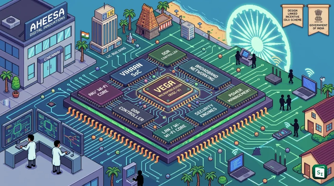
Chennai-based Aheesa Digital Innovations, a fabless semiconductor startup, has achieved first-pass silicon success with VIHAAN, the first domestically designed broadband networking System-on-Chip (SoC) in India. The chip is built around the indigenous 64-bit VEGA microprocessor developed by the Centre for Development of Advanced Computing (C-DAC), which offers a royalty-free RISC-V architecture. Its development was supported under the Design Linked Incentive (DLI) scheme of the central government, marking a significant step toward self-reliance in telecom silicon.
What Is the VIHAAN Chip?
VIHAAN is a System-on-Chip (SoC), a single silicon chip that integrates several components on one board. A SoC typically packs a processor, memory, and input-output circuits into a single package, which is why it can power small devices such as routers, phones, and television set-top boxes.
The chip was taped out on Republic Day (26 January 2026) and achieved first-pass silicon success on Independence Day (15 August 2026). The Ministry of Electronics and Information Technology (MeitY) announced the milestone, describing it as a key step toward taking the chip into commercial production. VIHAAN is designed for fibre broadband applications, meaning it will sit inside the fibre termination devices that deliver high-speed internet to homes and offices. The chip will now move toward production tape-out, which is targeted for 2027.
Aheesa designed the chip specifically to replace imported networking silicon. In a typical home, a fibre cable terminates in a small white box that contains a chip, a board, and antennas, most of which are currently sourced from outside India. VIHAAN is designed and developed entirely in India, offering an indigenous alternative for this critical component.
Understanding Tape-Out and First-Pass Silicon Success
Tape-out is the final stage of chip design, when the completed electronic design is sent to a semiconductor foundry for manufacturing. The term dates back to the era when design data was physically stored on magnetic tape and shipped to fabrication facilities.
First-pass silicon success means the chip worked correctly the very first time it was manufactured and tested, without needing a design correction. This is a rare achievement. Industry surveys suggest that first-silicon success rates have fallen to about 14 percent in recent years, as chip complexity keeps rising. A single error caught after tape-out is extremely expensive, since new masks and a fresh fabrication run are required. For an early-stage startup, clearing this milestone on the first attempt is a strong validation of the design team’s skills.
The VEGA Microprocessor: The Indian Core Inside
At the heart of VIHAAN lies the VEGA processor, a family of microprocessors designed by the Centre for Development of Advanced Computing (C-DAC). C-DAC is an autonomous scientific society under MeitY, established in March 1988 to build indigenous supercomputers after the United States refused to sell India a Cray supercomputer. Its headquarters are in Pune, and it built India’s first supercomputer, PARAM 8000, in 1991.
The VEGA series includes 32-bit and 64-bit single, dual, and quad-core processors based on the RISC-V instruction set architecture (ISA). RISC-V is an open, royalty-free instruction set that anyone can use and modify, which removes licensing costs and gives designers complete control over their chip. The name stands for reduced instruction set computer (RISC) and the Roman numeral V, meaning the fifth generation of the RISC family.
The VEGA processors were developed under the Microprocessor Development Programme and the Digital India RISC-V (DIR-V) programme, which the government launched in April 2022 to create next-generation indigenous microprocessors. The DIR-V programme aims to make India a global RISC-V talent hub and a supplier of RISC-V SoCs for servers, mobile devices, automotive, and Internet of Things applications. C-DAC has also fabricated its own VEGA-based chips, including the THEJAS64, a 64-bit single-core SoC fabricated at the Semi-Conductor Laboratory (SCL) in Chandigarh.
Because VIHAAN uses the VEGA core, it inherits a royalty-free and customizable architecture. This is strategically important. It means the chip design is free of foreign licensing costs, and India retains full ownership of the intellectual property inside its own networking infrastructure.
The Design Linked Incentive Scheme: Fuel for Designers
VIHAAN’s development was supported under the Design Linked Incentive (DLI) scheme, a central government programme under the Semicon India Programme. The scheme was announced by MeitY in January 2022 with an outlay of around ₹1,000 crore. Its purpose is to offset the disadvantages faced by Indian companies in semiconductor design and to strengthen the chip design ecosystem in the country.
The DLI scheme is open to domestic companies, startups, and Micro, Small and Medium Enterprises (MSMEs) engaged in semiconductor design or semiconductor-linked design. C-DAC serves as the nodal agency responsible for implementing the scheme. Companies that claim incentives must retain domestic status, meaning more than 50 percent of their capital must remain beneficially owned by resident Indian citizens or Indian companies, for at least three years.
How the DLI Scheme Works
The scheme provides support in three broad ways:
| Component | What It Offers |
|---|---|
| Chip design infrastructure support | Gives approved companies access to industry-standard Electronic Design Automation (EDA) tools, the software used to design and verify chips |
| Product Design Linked Incentive | Reimburses up to 50 percent of eligible expenditure, capped at ₹15 crore per project, covering design, testing, and demonstration of products ready for volume production |
| Deployment Linked Incentive | Rewards commercialization by offering 4 to 6 percent of net sales turnover over five years, capped at ₹30 crore per applicant |
The DLI scheme is one part of the larger Semicon India Programme, which was launched in December 2021 with a total outlay of ₹76,000 crore. The government has since approved Semicon 2.0 in July 2026 with an outlay of ₹1,27,500 crore to expand support across the entire semiconductor value chain, including design, fabrication, packaging, materials, and talent development.
Why an Indigenous Fibre Broadband Chip Matters for India
India’s digital economy depends heavily on fibre broadband infrastructure. Networks such as BharatNet, which aims to connect more than 2.5 lakh gram panchayats with optical fibre, and the rapid rollout of 5G and 6G services all rely on network equipment built around semiconductors.
The white boxes on walls and poles, where fibre cables terminate, contain chips that are almost entirely imported today. Aheesa founder and CEO Sridharan Mani has explained that in a typical home or office, the chip inside the fibre termination box, the board, and even the antennas usually come from outside India. VIHAAN replaces that imported chip with one designed and developed entirely in India.
This matters for two reasons. First, economic value: semiconductor chip design contributes up to 50 percent of overall value addition in the semiconductor value chain and accounts for roughly 15 to 35 percent of the bill of materials cost of electronic products. Second, strategic security: India currently imports around 90 to 95 percent of the semiconductors it consumes, and much of that demand flows from China, Taiwan, and other countries. A NITI Aayog roadmap released in May 2026 warned that annual semiconductor import costs could climb toward $240 billion by 2035 if current trends continue, making self-reliance in critical chips a matter of national security as much as economics.
A Growing Semiconductor Design Ecosystem
VIHAAN is not an isolated success. Companies supported under the DLI scheme have cumulatively achieved more than 30 chip design tape-outs across various foundries and have raised more than $100 million in venture capital funding, according to the government. This reflects a maturing design ecosystem in which Indian startups are moving from idea to silicon.
Aheesa itself has been scaling rapidly. The company, established in 2021, raised about ₹40 crore earlier this year from the Tamil Nadu Infrastructure Fund Management Corporation (TNIFMC) through the Tamil Nadu Emerging Sector Seed Fund (TNESSF) and other private investors. In August 2026, it signed a memorandum of understanding with Guidance, the investment promotion agency of the Tamil Nadu government, for a proposed semiconductor design, R&D, and product engineering centre in Chennai. The centre entails an investment of around ₹250 crore and is expected to create more than 300 jobs.
These developments sit within the larger story of India’s semiconductor push. Twelve manufacturing units have been approved with a cumulative investment of over ₹1.64 lakh crore, and three companies, Micron, Kaynes, and CG Semi, have already started commercial production at their facilities in Sanand, Gujarat. India’s own fabless segment benefits from a deep talent pool, as the country is home to about 20 percent of the world’s semiconductor design engineers.
The Way Forward
VIHAAN will now proceed toward production tape-out, targeted for 2027. If commercial production succeeds, the chip could find its way into fibre broadband equipment used by telecom operators across India, reducing dependence on imported networking silicon.
The broader vision is ambitious. Semicon 2.0 is expected to catalyse investments of around ₹4 lakh crore, generate semiconductor and electronics production worth ₹2 lakh crore, and boost exports by approximately ₹1 lakh crore in the coming years. For startups like Aheesa, the challenge now shifts from design to commercialization: winning customer contracts, meeting telecom-grade reliability standards, and proving the chip in real networks.
Still, the milestone carries a symbolic weight of its own. A chip designed in Chennai, around a processor designed in Pune, passing its first silicon test on Independence Day, is a concrete demonstration of India’s ability to move from consuming chips to creating them.
Key Takeaways
- VIHAAN, designed by Chennai-based Aheesa Digital Innovations, is the first domestically designed broadband networking System-on-Chip (SoC) in India.
- The chip was taped out on 26 January 2026 (Republic Day) and achieved first-pass silicon success on 15 August 2026 (Independence Day), with production tape-out targeted for 2027.
- VIHAAN is built on the VEGA microprocessor, a 64-bit processor developed by C-DAC under the Digital India RISC-V (DIR-V) programme, based on the royalty-free RISC-V architecture.
- C-DAC, established in March 1988 and headquartered in Pune, is the nodal agency for implementing the Design Linked Incentive (DLI) scheme, announced by MeitY in January 2022 with an outlay of about ₹1,000 crore.
- DLI-backed companies have achieved more than 30 chip design tape-outs and raised over $100 million in venture capital funding.
- The government approved Semicon 2.0 in July 2026 with an outlay of ₹1,27,500 crore to expand support across the entire semiconductor value chain.